No products in the cart.
AdValue Technology, in collaboration with Fraunhofer IKTS, proudly offers a comprehensive and unique thick-film paste system optimized for aluminum nitride (AlN) ceramics.
Our thick-film paste series deliver standardized and tested pastes ideal for applications in microelectronics, microsystems, and sensor technologies. These pastes are engineered for consistent film thicknesses, stable film properties, and are eco-friendly, resource-efficient, and fully compliant with RoHS II and REACH regulations.
In addition to our standard pastes, we also have the ability to offer custom-formulated pastes – specially researched and developed to meet the specific requirements of our customers.
Backed by our robust quality assurance system aligned with ISO 9000 standards, we ensure reliable performance and consistent results with each batch.
Explore our paste categories below. Click the links to learn more about each product.
Please feel free to contact us to discuss your application and request a quote.
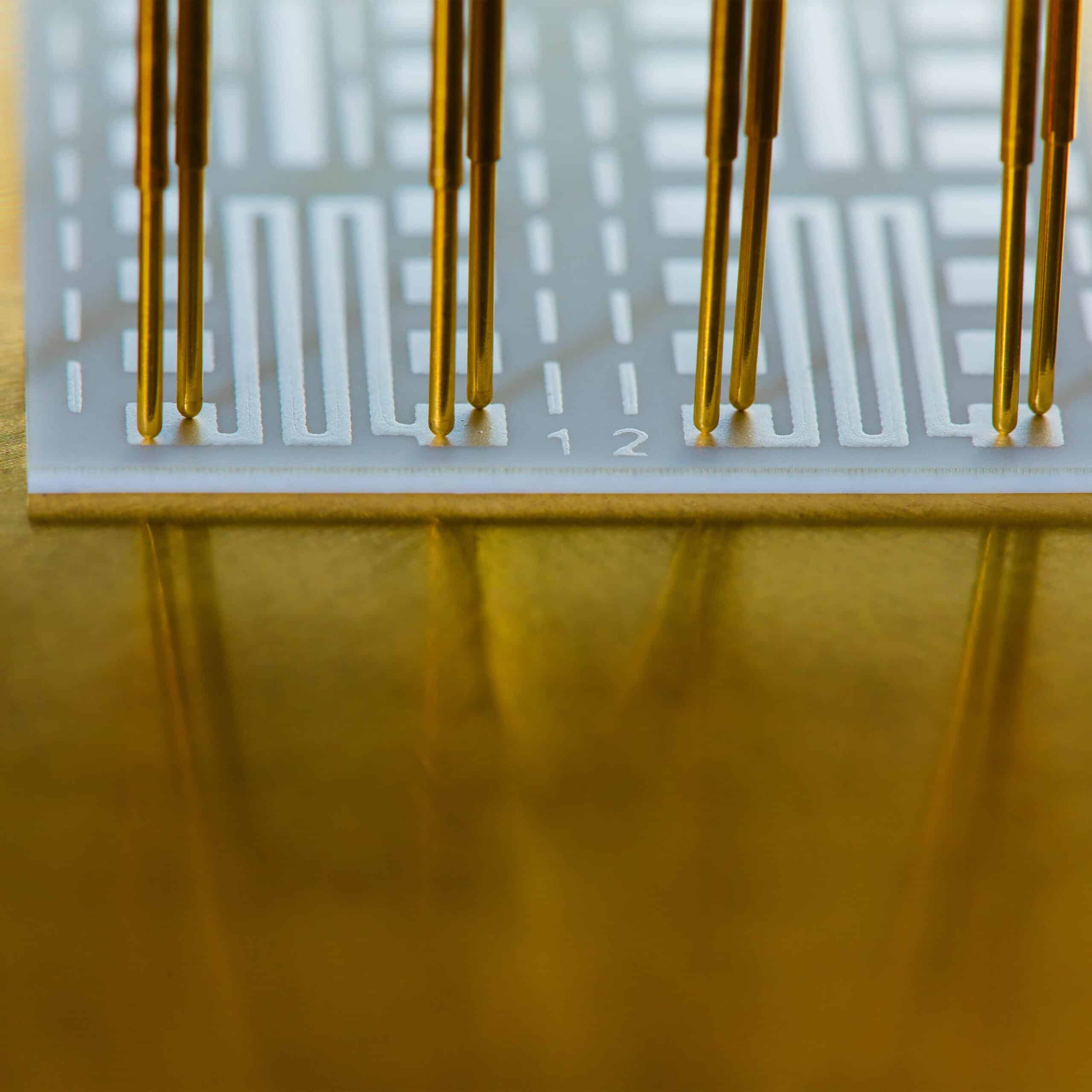
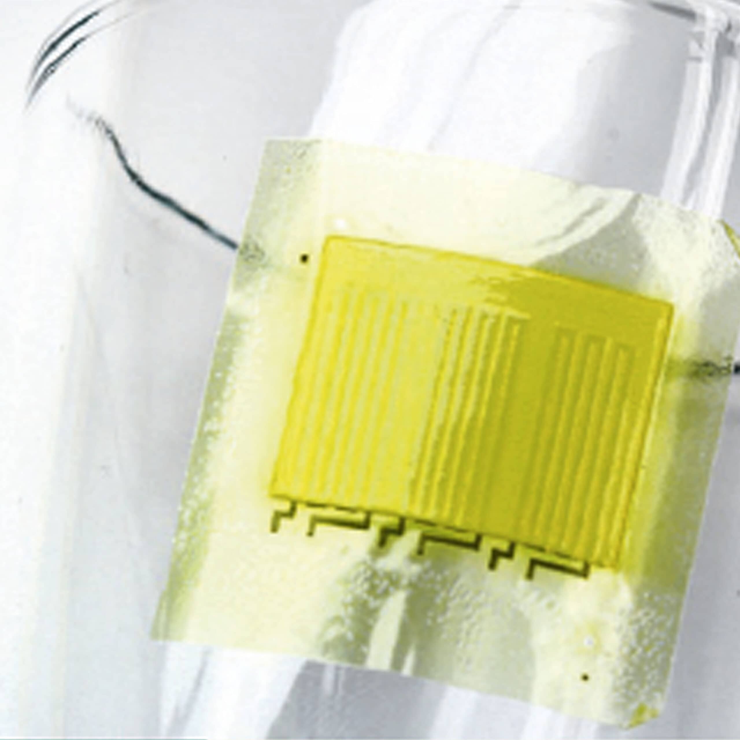
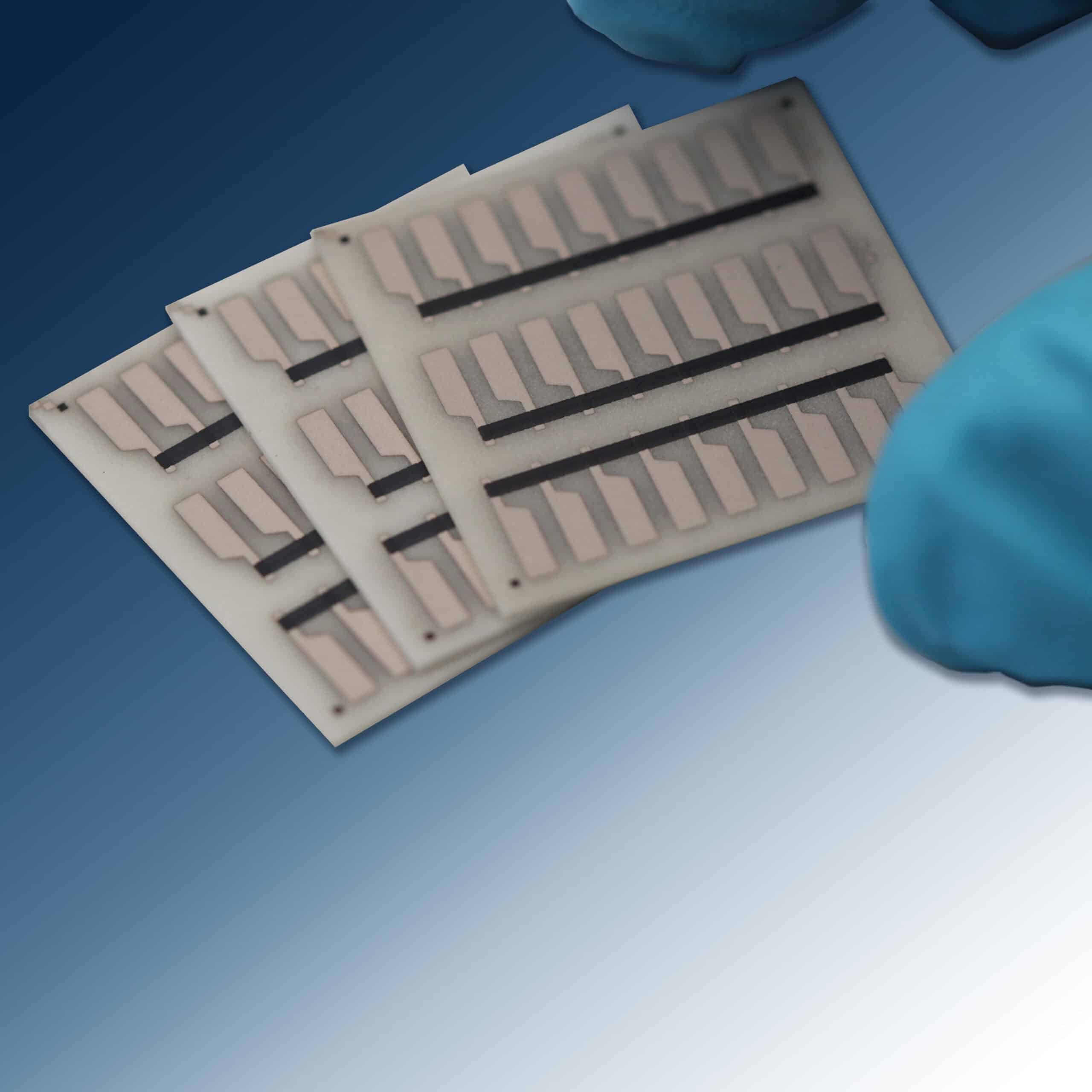
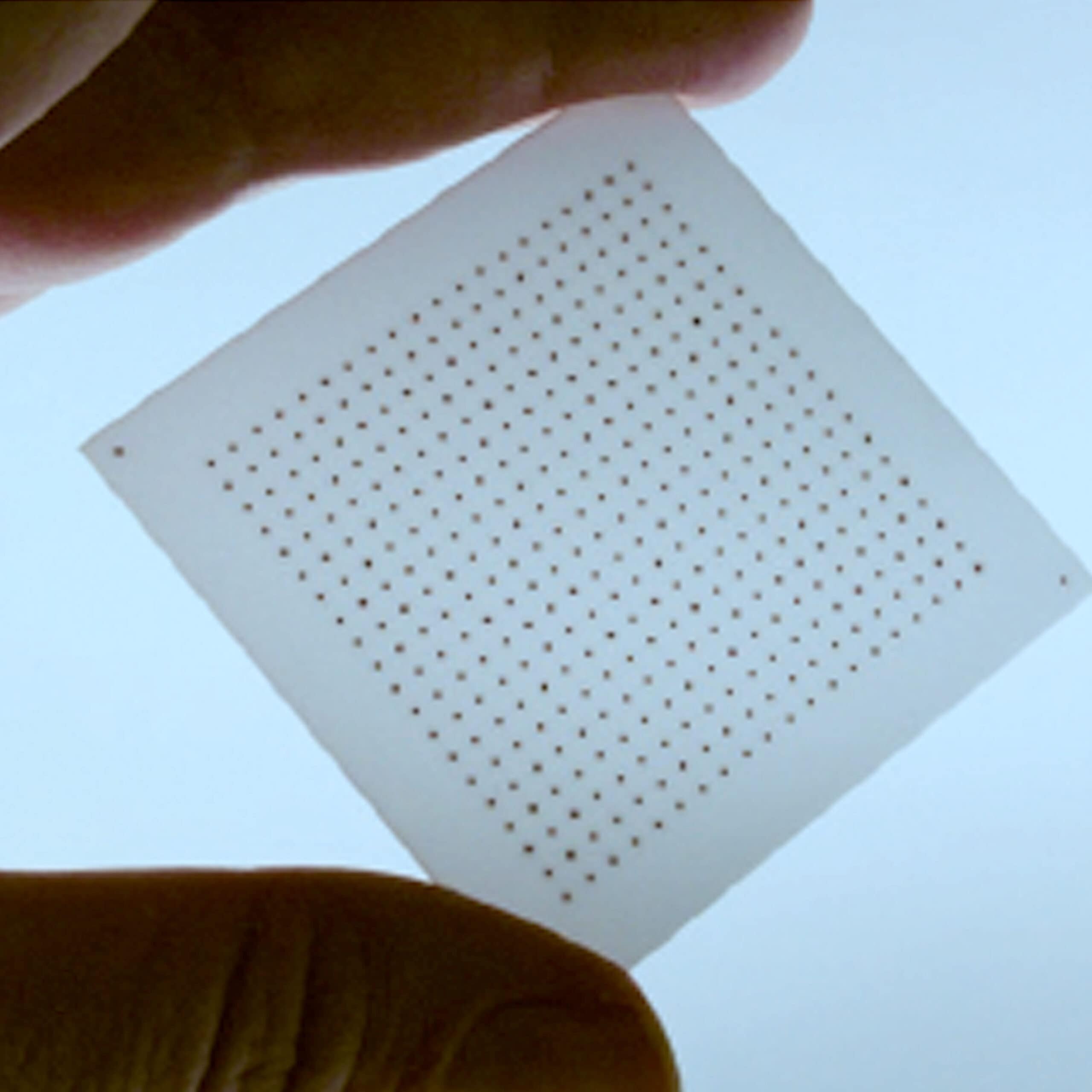
Thick film pastes are materials that have been specially formulated for use in printing conductive, resistive, or insulating layers onto ceramic substrates. They are applied using screen-printing techniques and then fired at high temperatures to create durable, precise electronic circuits and components.
The main difference between the two types of film materials is the application method and layer thickness. Thick film pastes are screen-printed and fired, yielding robust layers between 10 to 25 micrometers. On the other hand, thin film materials are deposited using vacuum-based techniques (like sputtering) for thinner, more uniform layers. Between the two material types, thick film technology is generally more cost-effective and better suited for high-power and rugged applications.
AdValue Technology’s thick film pastes are specifically optimized for Aluminum Nitride (AlN) ceramics, a substrate prized for its excellent thermal conductivity and electrical insulation properties. AlN substrates are the preferred choice in high-power electronics where heat dissipation is critical in preventing mechanical stress and premature failure.
Aluminum Nitride is a standout substrate material for several reasons. It offers exceptionally high thermal conductivity, which makes it ideal for high-power applications where heat needs to move away from the circuit fast. It’s also an excellent electrical insulator, chemically stable, and mechanically strong.
AdValue Technology offers four core categories of thick film pastes that each serve a distinct function in electronic circuit fabrication. These include the following:
Conductor paste is the foundation of any thick film circuit. This material is screen-printed onto a substrate to create electrically conductive traces, pads, and interconnections. Once fired, it forms a solid metallic layer that carries electrical current efficiently, and is a crucial component in applications like power modules, sensors, and hybrid microelectronics that require reliable transmission.
Resistor paste lets engineers print precise resistive elements directly onto the ceramic substrate, offering a more compact and integrated approach than placing discrete resistor components. After firing, the resistor paste forms a stable film with controlled resistance values, which is critical for sensor calibration, voltage division, and signal conditioning in microelectronic devices.
Glass paste acts as a dielectric and protective layer within the circuit. It insulates conductive layers from one another, protects underlying films from environmental exposure, and improves the mechanical durability of the finished assembly. In multilayer circuit designs, glass paste is what makes stacking multiple functional layers possible without short circuits or interference.
Via filling paste is used when your circuit design requires electrical connections between different layers of a substrate or board. The paste is pressed into drilled or laser-cut holes (vias) in the ceramic, and after firing, it creates a solid, conductive path that bridges the layers. This is especially important in compact, multilayer microelectronic assemblies where space is tight.
Thick film pastes are utilized across a variety of high-performance industries, including:
Here’s a quick look at where these pastes make the biggest impact:
| Application | Paste Type Used |
|---|---|
| Power electronics and modules | Conductor, Resistor, Glass, Via Filling where multilayer substrates are used |
| Temperature and pressure sensors | Resistor, Conductor, Glass |
| Multilayer hybrid circuits | Conductor, Glass, Via Filling, Resistor |
| Insulation and passivation layers | Glass |
| Microelectronic assemblies | All four paste types |
| Gas sensing devices | Resistor, Conductor, Glass |
| Medical diagnostic equipment | Conductor, Resistor, Glass, Via Filling where multilayer substrates are used |
The combination of AlN substrates and AdValue Technology’s thick film paste system is specifically engineered for high-power applications. AlN’s superior thermal conductivity means heat dissipates efficiently, and the paste system is formulated to maintain stable performance under elevated temperatures and demanding electrical loads. It’s a pairing designed for reliability where it counts most.
All thick film pastes offered by AdValue Technology are standardized and rigorously tested before they reach your hands. They’re engineered for consistent film thicknesses and stable film properties from batch to batch. That kind of repeatability is critical when you’re manufacturing precision electronics at scale.
AdValue Technology maintains a robust quality assurance system aligned with ISO 9000 standards. Every paste batch goes through strict quality control to ensure performance consistency, reliability, and conformity to specification.
AdValue Technology’s thick film pastes are fully compliant with both RoHS II and REACH regulations. This matters enormously for manufacturers selling into European and global markets where environmental and safety compliance isn’t optional.
RoHS II (Restriction of Hazardous Substances Directive II) restricts the use of specific hazardous materials, such as lead, mercury, and cadmium, in electrical and electronic equipment. A RoHS II-compliant paste means it does not contain these restricted substances above permitted thresholds, making it safer for both end users and the environment.
REACH (Registration, Evaluation, Authorisation and Restriction of Chemicals) is a European Union regulation that governs the use of chemical substances in products. REACH compliance means that AdValue Technology’s pastes have been assessed for chemical safety and do not contain substances of very high concern (SVHCs) above the allowable limits.
The thick film paste system developed with Fraunhofer IKTS is designed to be eco-friendly and resource-efficient. This reflects a commitment not just to performance, but to sustainable materials practices that align with modern environmental expectations in electronics manufacturing.
AdValue Technology collaborates with Fraunhofer IKTS, a globally recognized research institute specializing in ceramic technologies and hybrid microsystems. This partnership brings cutting-edge research and development directly into AdValue Technology’s product lineup, giving customers access to pastes that reflect the latest advancements in thick film science.
AdValue Technology offers custom-formulated pastes specially researched and developed to meet specific customer requirements. Whether you need a unique viscosity, firing profile, conductivity level, or substrate compatibility, our engineering team can work with you to develop a solution tailored to your application.
Reach out to the AdValue Technology team directly with your project requirements. The more detail you can provide about your substrate, target application, processing temperatures, and performance requirements, the better we can tailor a solution for you. Contact options are listed at the end of this document.
Standard items typically ship within 2–3 weeks. For custom formulations or larger volume orders, lead times will vary depending on the scope of the development work involved.
AdValue Technology is a full-service specialty materials supplier. Alongside thick film pastes, we offer: